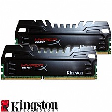
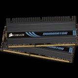
SPECIFICATIONS
CL(IDD) 9 cycles
Row Cycle Time (tRCmin) 49.5ns (min.)
Refresh to Active/Refresh 260ns (min.)
Command Time (tRFCmin)
Row Active Time (tRASmin) 36ns (min.)
Maximum Operating Power 2.460 W* (per module)
UL Rating 94 V - 0
Operating Temperature 0o C to 85o C
Storage Temperature -55o C to +100o C
*Power will vary depending on the SDRAM used.
FEATURES
• JEDEC
standard 1.5V (1.425V ~ 1.575V) Power Supply
• VDDQ =
1.5V (1.425V ~ 1.575V)
• 667MHz fCK
for 1333Mb/sec/pin
• 8
independent internal bank
• Programmable
CAS Latency: 9, 8, 7, 6
• Posted CAS
• Programmable
Additive Latency: 0, CL - 2, or CL - 1 clock
• Programmable
CAS Write Latency(CWL) = 7 (DDR3-1333)
• 8-bit
pre-fetch
• Burst
Length: 8 (Interleave without any limit, sequential with
starting address “000” only), 4 with tCCD = 4
which does not
allow seamless read or write [either on the
fly using A12 or
MRS]
• Bi-directional
Differential Data Strobe
• Internal(self)
calibration : Internal self calibration through ZQ
pin (RZQ : 240 ohm ± 1%)
• On Die
Termination using ODT pin
• Average
Refresh Period 7.8us at lower than TCASE 85°C,
3.9us at 85°C < TCASE < 95°C
• Asynchronous
Reset
• PCB : Height
1.827” (46.41mm) w/ heatsink, double sided
component